A4 Size PCB Layout: The Ultimate Guide for Designers Pcb layout design tutorial pcb design steps & complete guide maximizing
If you are searching about PCB Layers: Everything You Need to Know you've came to the right place. We have 25 Pics about PCB Layers: Everything You Need to Know like The Ultimate Guide to PCB Layout Design - MOKO, pcb layout design tutorial Pcb design steps & complete guide Maximizing and also Ultimate Guide To Pcb Layout Design Considerations Mcl Images. Here it is:
PCB Layers: Everything You Need To Know
 www.mktpcb.com
pcb
The Basics Of Schematics: Understanding Circuit Diagrams And Symbols
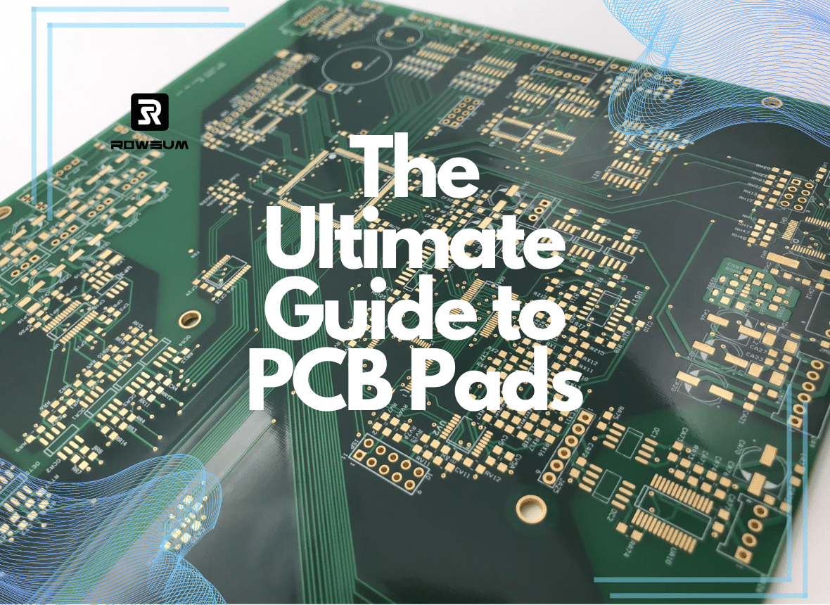 www.rowsum.com
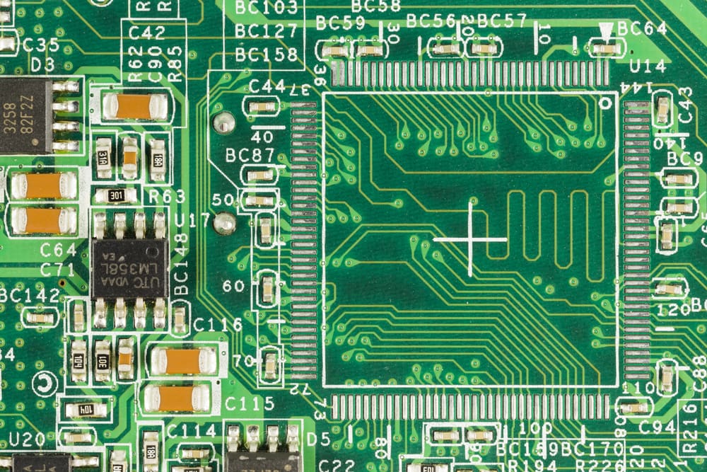
Pcb Design Course Nptel From Beginner To Expert: The Ultimate Pcb
 pcbhouses.pages.dev
The Ultimate Arduino PCB Guide - Everything You Need To Know - PCBA
 www.pcba-manufacturers.com
PCB Layers: The Ultimate FAQ Guide
 www.wellpcb.com
pcb panel standard layers circuit enig pcbs proto prototype fabrication hasl wellpcb ourpcb array breadboard plating
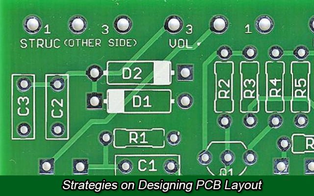
Ultimate Guide To Pcb Layout Design Considerations Mcl Images
 www.tpsearchtool.com
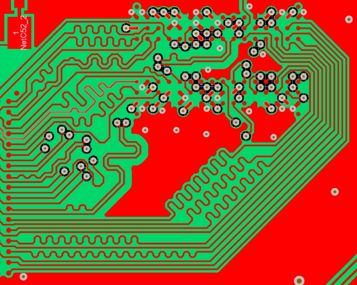
PCB Layout: A Comprehensive Guide
 www.wevolver.com
Ultimate Guide To Pcb Layout Design Considerations Mcl Images
 www.tpsearchtool.com
Introducing Layout: Your Ultimate PCB Layout Solution! - Excel Circuit
 www.excelcircuit.com
The Ultimate Guide To Pcb Hardware - Vrogue.co
 www.vrogue.co
O Melhor Guia Para Design De Layout De PCB - MOKO
 www.mokotechnology.com
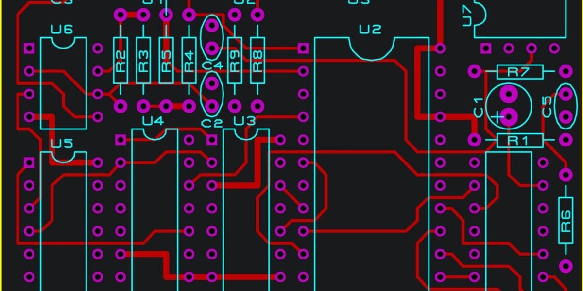
Pcb Layout Design Tutorial Pcb Design Steps & Complete Guide Maximizing
 pcblites.pages.dev
Pcb Layout Guidelines For Design - Vrogue.co
 www.vrogue.co
PCB Design Layout Guidelines For Engineers | Advanced PCB Design Blog
 resources.pcb.cadence.com
PCB Layout Design - ESP32-C3 - — ESP Hardware Design Guidelines Latest
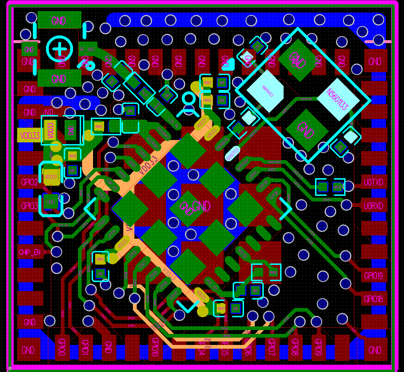 docs.espressif.com
Pcb Board Design Guide At Santiago Vanmatre Blog
 storage.googleapis.com
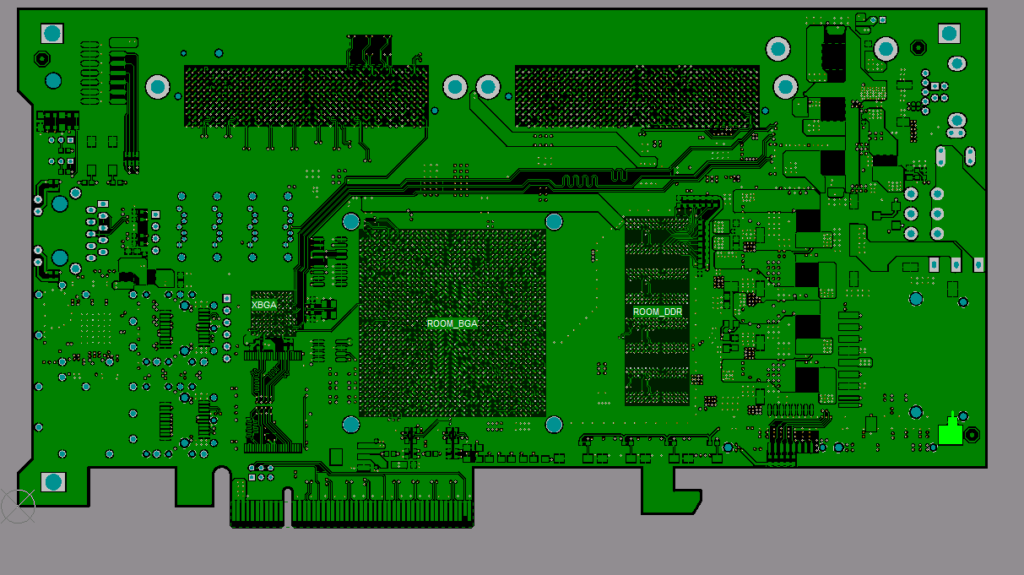
The Ultimate Guide To PCB Layout Design - MOKO
 www.mokotechnology.com
Ultimate Guide To Pcb Layout Design Considerations Mcl Images
 www.tpsearchtool.com
Understanding CTE In PCB: Challenges And Solutions - TechSparks
 www.tech-sparks.com
How To Print PCB On A4 Size Paper / Print Exact Size PCB On A4 Size
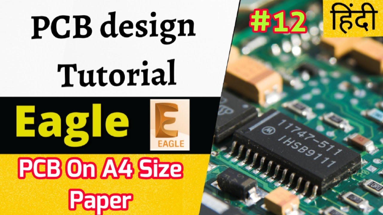 www.youtube.com
Pcb Layout Design Tutorial Pcb Design Steps & Complete Guide Maximizing
A Detailed Guide To PCB Layout Design - IBE Electronics
 www.pcbaaa.com
Tented Via: The Ultimate Guide To PCB Design And Manufacturing Techniques
 www.wevolver.com
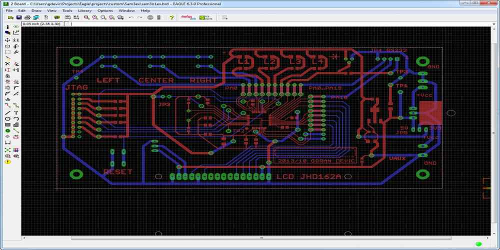
An Ultimate Guide To PCB Wiring And Layout
 hillmancurtis.com
A Detailed Guide To PCB Layout Design - IBE Electronics
 www.pcbaaa.com
Pcb panel standard layers circuit enig pcbs proto prototype fabrication hasl wellpcb ourpcb array breadboard plating. Pcb board design guide at santiago vanmatre blog. Tented via: the ultimate guide to pcb design and manufacturing techniques