PCIe PCB Layout Guidelines: Essential Tips for Designers A detailed guide to pcb layout design
If you are looking for PCB layout rules for PCIE Pcb design basics: from schematic to board you've visit to the right place. We have 25 Images about PCB layout rules for PCIE Pcb design basics: from schematic to board like PCIe Gen 6: PCB Design Essentials | EMA Design Automation, Designing PCIe interfaces and extenders « Adafruit Industries – Makers and also PCIe Gen 6: PCB Design Essentials | EMA Design Automation. Read more:
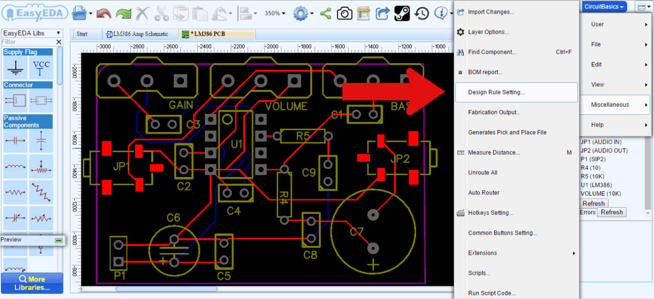
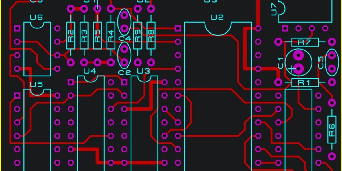
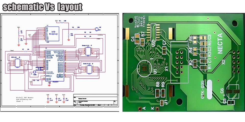
PCB Layout Rules For PCIE Pcb Design Basics: From Schematic To Board
 pcblites.pages.dev
PCIE-PCB设计规范!(建议收藏)-CSDN博客
PCIe In PCB Design: Layout And Routing Guidelines | Blog | Altium Designer
PCIe In PCB Design: Layout And Routing Guidelines | Blog | Altium Designer
 resources.altium.com
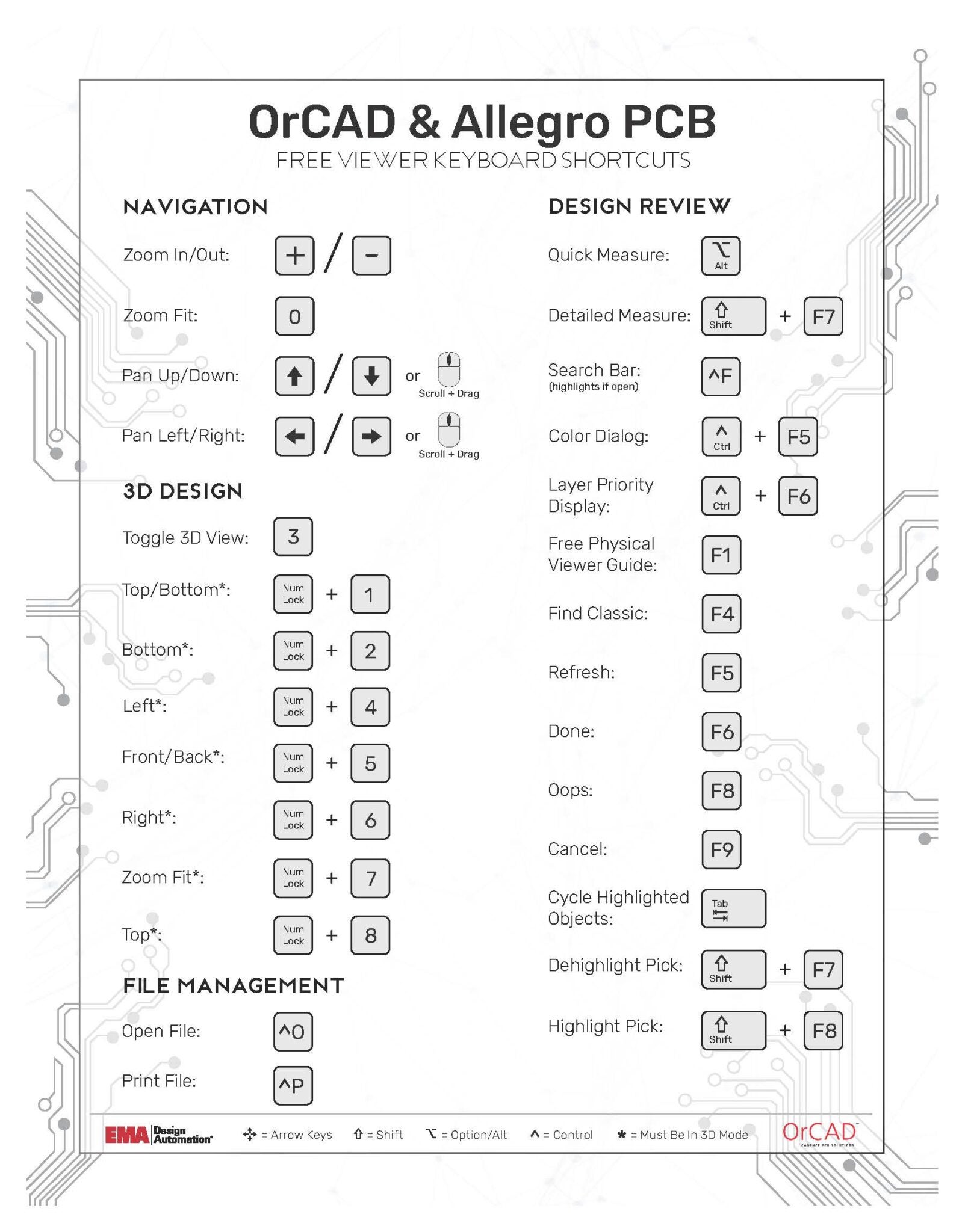
PCIe Gen 6: PCB Design Essentials | EMA Design Automation
 www.ema-eda.com
Pcb Design Layout Guidelines Pcb Layout Guidelines For Design 21+ Pcb
 pcbhouse.pages.dev
PCIe Gen 6: PCB Design Essentials | EMA Design Automation
 www.ema-eda.com
Pcie Pcb Layout Guidelines Pc & Pci Cards
 pcbdesigns.netlify.app
A Detailed Guide To PCB Layout Design - IBE Electronics
 www.pcbaaa.com
PCIe Gen 6: PCB Design Essentials | EMA Design Automation
 www.ema-eda.com
PCB Layout Rules For PCIE Pcb Design Basics: From Schematic To Board
 pcblites.pages.dev
PCIe Gen 6: PCB Design Essentials | EMA Design Automation
 www.ema-eda.com
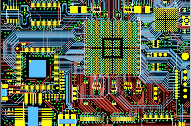
How To Design A PCB Layout: A Comprehensive Guide
 www.wevolver.com
Pcie Pcb Routing Rules - PCB Designs
 pcbdesignsdl.blogspot.com
design pcb pcie routing board circuit rules pci services layout electrical ok stack engineering does look quote
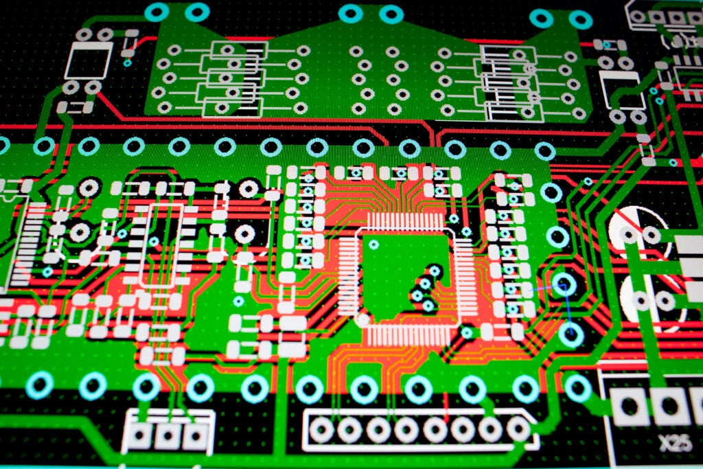
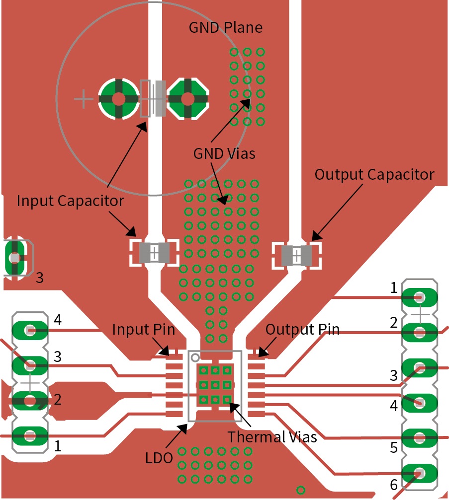
PCB Design Guidelines For High Current Applications - HardwareBee
 hardwarebee.com
pcb design layout guide high guidelines electronic ultimate process
PCIe Routing Guidelines & Best Practices - Free Online PCB CAD Library
 www.ultralibrarian.com
PCB Layout Rules For PCIE, SATA, LAN, LVDS, USB, SDVO,
 www.fedevel.com
Quickly Complete Panelization With CAM350 - TechSparks
 www.tech-sparks.com
PCIe Gen 6: PCB Design Essentials | EMA Design Automation
 www.ema-eda.com
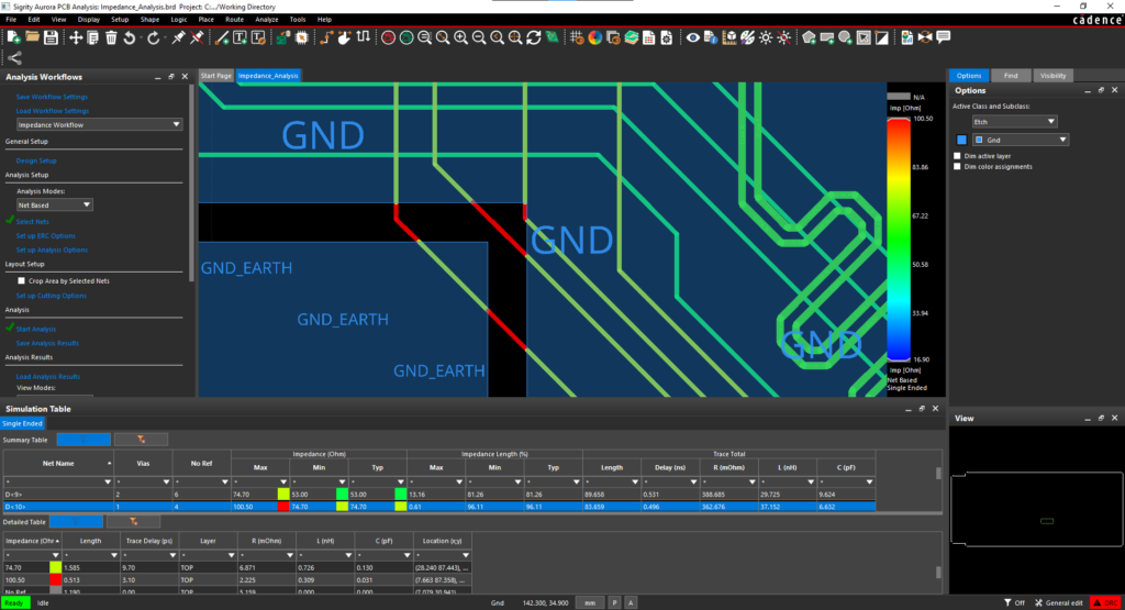
PCIe Routing Guidelines: Overview | EMA Design Automation
 www.ema-eda.com
Designing PCIe Interfaces And Extenders « Adafruit Industries – Makers
 blog.adafruit.com
Rolling Your Own PCIe Bifurcation Riser – Matt's Tech Pages
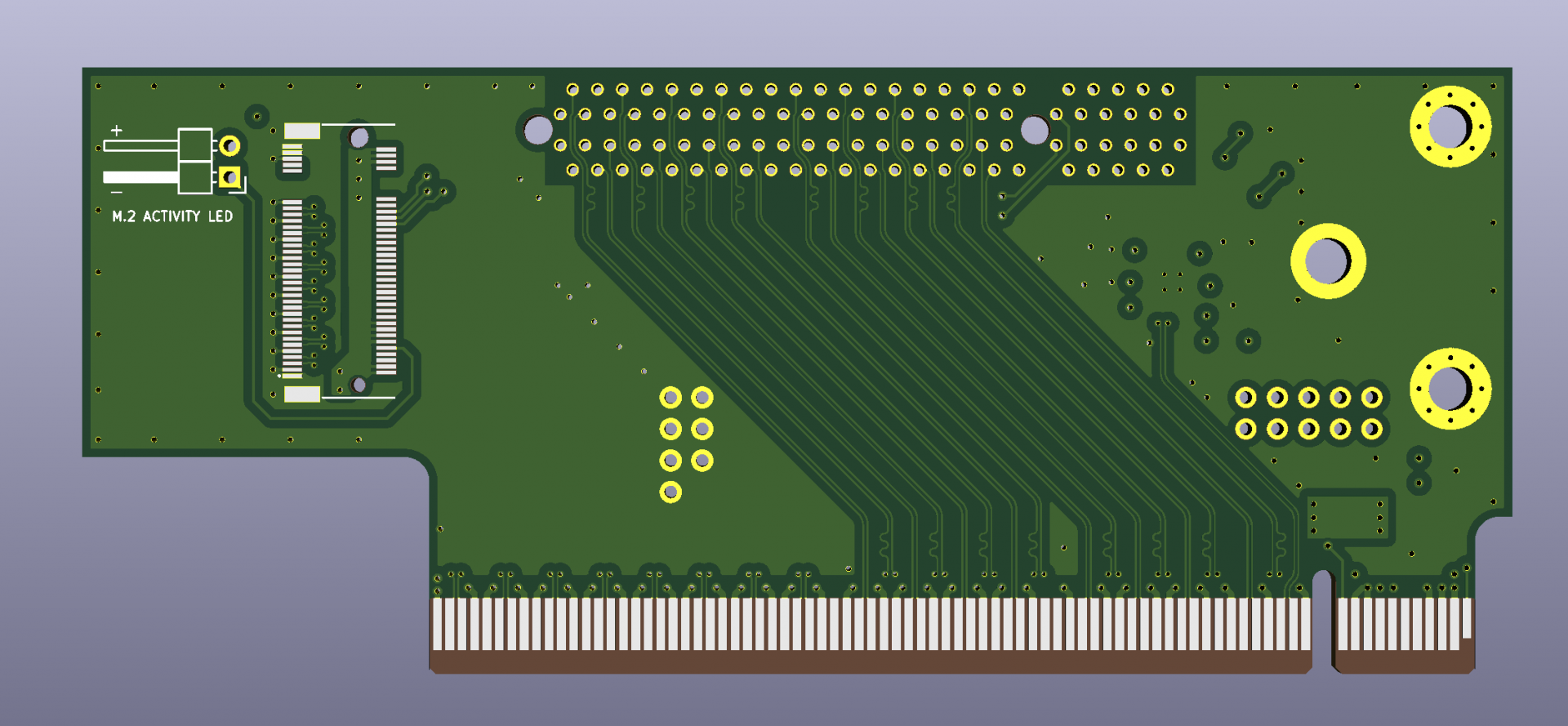 www.mattmillman.com
PCB Layout Rules For PCIE Pcb Design Basics: From Schematic To Board
 pcblites.pages.dev
PCI Express 设计指南(PCB板) - Jinzi - 博客园
 www.cnblogs.com
PCIe Gen 6: PCB Design Essentials | EMA Design Automation
 www.ema-eda.com
Pcie gen 6: pcb design essentials. Pcie gen 6: pcb design essentials. Quickly complete panelization with cam350