PCB Board Design Tutorial: Learn to Create Professional Layouts! How to design a pcb layout
If you are searching about PCB Design Tutorial_56 Oracd Pcb Editor Board Fiducial Placement - YouTube you've came to the right page. We have 25 Pictures about PCB Design Tutorial_56 Oracd Pcb Editor Board Fiducial Placement - YouTube like PCB Design Tutorial Using EasyEDA & JLCPCB | PCB Designing, PCB Design Tutorial with DipTrace for beginners - PCB Design Tutorial and also PCB Design Tutorial with DipTrace for beginners - PCB Design Tutorial. Here it is:
PCB Design Tutorial_56 Oracd Pcb Editor Board Fiducial Placement - YouTube
 www.youtube.com
pcb fiducial
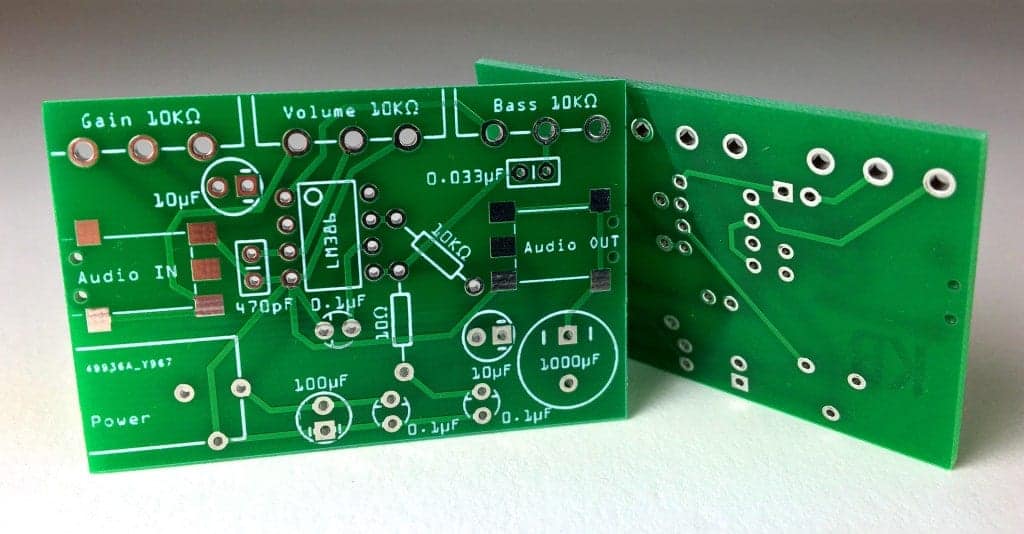
Pcb Board Design Guide At Santiago Vanmatre Blog
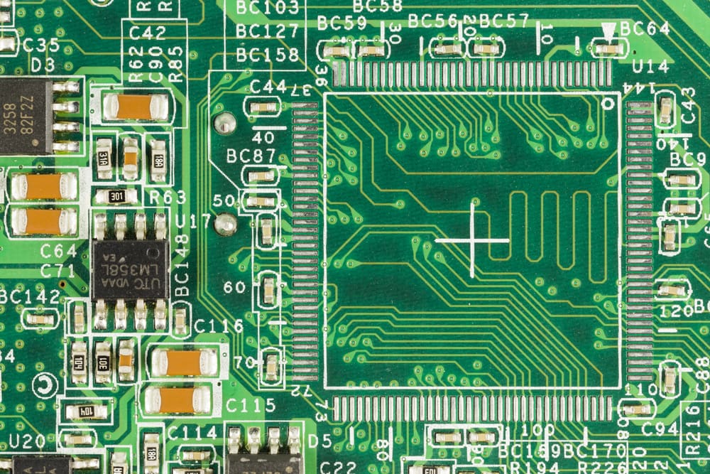 storage.googleapis.com
Altium Pcb Design Tutorial Pdf
 pcb-design.pages.dev
How To Make Pcb From Schematics
 manualrepinement.z14.web.core.windows.net
Pcb Design Circuit Diagram - Designing Your Own Pcb With Proteus Easy
 afiqchedeyyyy.blogspot.com
pcb electricaltechnology proteus easy
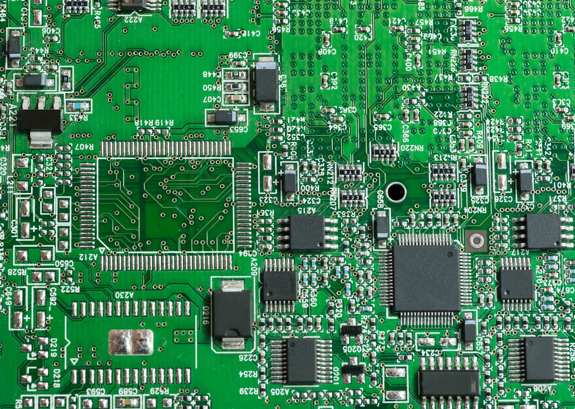
High Frequency Pcb Board Design - PCB Manufacturing And PCB Assembly
 www.andwinpcb.com
Custom Pcb Board Design Professional Custom Pcb Board Assembly Design
 pcbways.pages.dev
PCB Design Tutorial With DipTrace For Beginners - PCB Design Tutorial
 www.pcbway.com
PCB Design Tutorial For Eagle
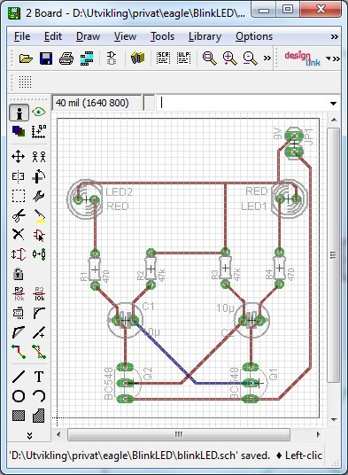 www.build-electronic-circuits.com
pcb tutorial design eagle layout create circuits electronic build electronics routing board shape erc drc errors run check
PCB Design Tutorial Using EasyEDA & JLCPCB | PCB Designing
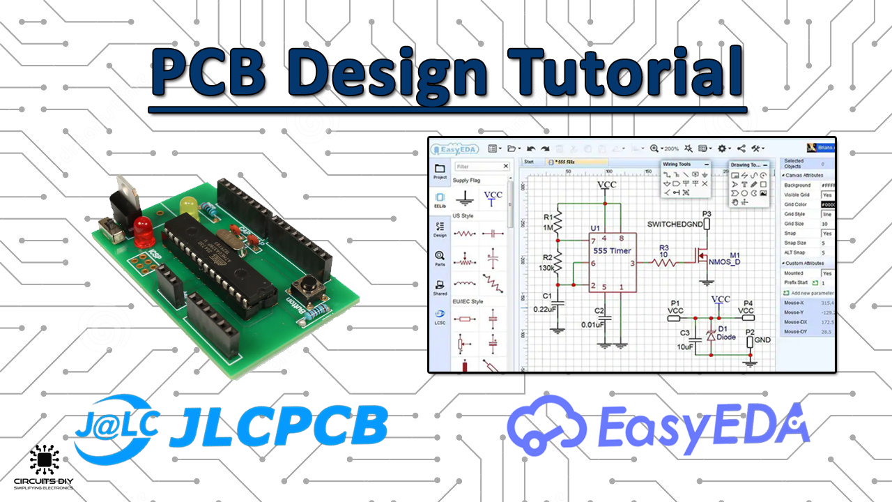 circuits-diy.com
pcb design easyeda tutorial jlcpcb designing using
Schematic Diagram To Pcb Layout Converter
 www.circuitdiagram.co
Altium Designer Pcb Layout Tutorial Pdf
 circuitwiringnosily77.z21.web.core.windows.net
How To Design A PCB Layout - Circuit Basics
 www.circuitbasics.com
pcb custom design layout circuit make basics
Eagle Pcb Design Software
 guidemanualtheek.z21.web.core.windows.net
Circuit Board Schematics - Circuit Diagram
 www.circuitdiagram.co
How To Design Your Own PCB [ SPRINT LAYOUT TUTORIAL ] - YouTube
![How to Design your own PCB [ SPRINT LAYOUT TUTORIAL ] - YouTube](https://i.ytimg.com/vi/wreWL6lfs5c/maxresdefault.jpg) www.youtube.com
www.youtube.com
layout sprint pcb design own tutorial
Using EAGLE: Board Layout - SparkFun Learn
 learn.sparkfun.com
eagle board layout sparkfun using pcb electronics learn make circuits tutorial vias job better than example if do can see
4 Layer PCB Layout Tutorial,Stack-up Design,and Cost Of Manufacturing
 www.raypcb.com
pcb layer design stack stackup up tutorial layout board comparison cost
How To Design PCB Board: A Step-by-step Guide For PCB Design
 www.pcbasic.com
Step-by-step Cadence PCB Design Tutorial - RayPCB
 www.raypcb.com
10 Essential PCB Design Software Tutorials For Beginners
 tryvary.com
How To Pcb Design Tutorial At Denise Singleton Blog
 storage.googleapis.com
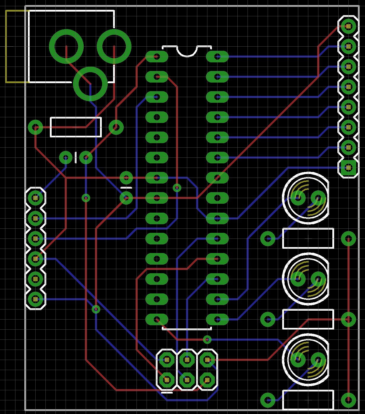
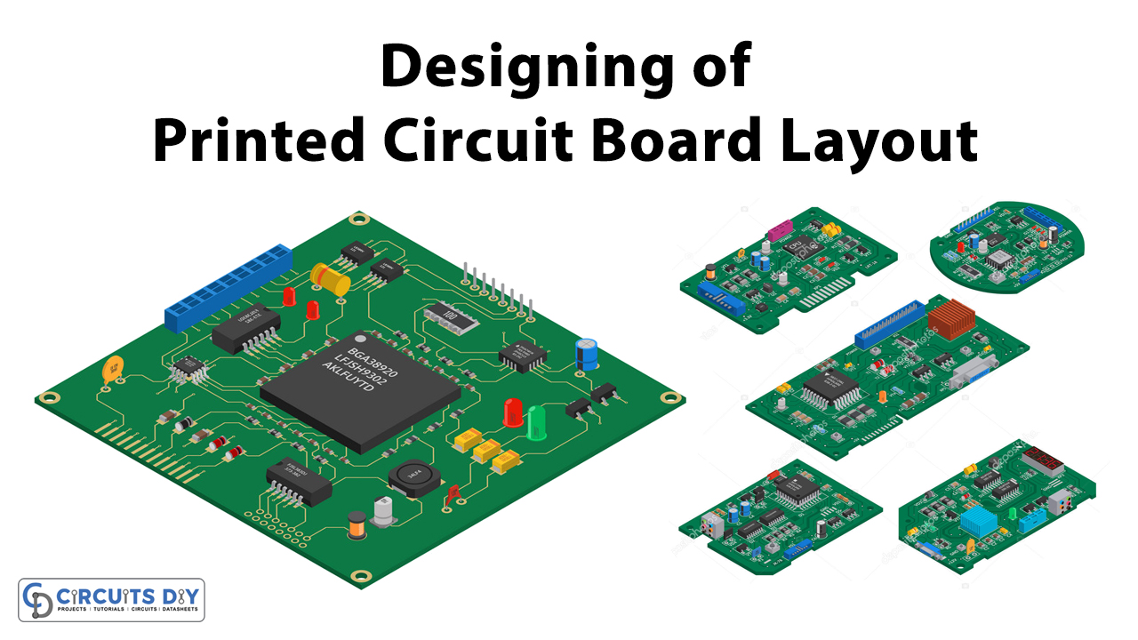
Designing Of Printed Circuit Board Layout | PCB | Maker Pro
 maker.pro
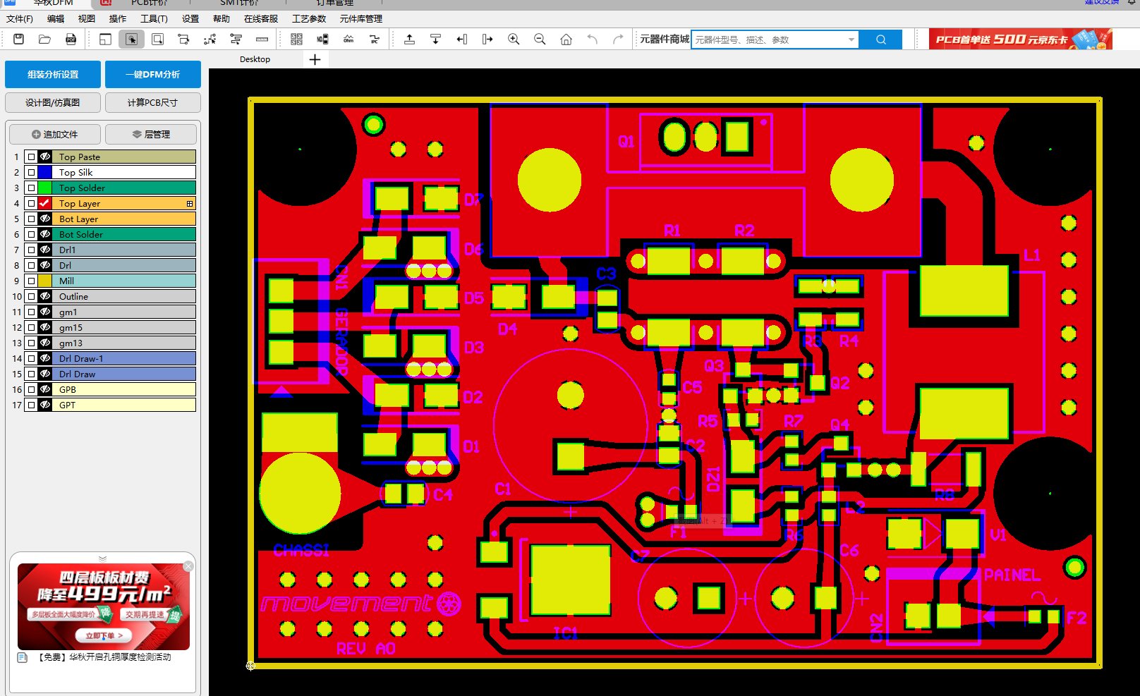
PCB Layout Design Par Siemens | PADS Professional | Cadlog
 www.cadlog.fr
Pcb Design Job Board Circuit Board Design
 pcbways.pages.dev
Altium pcb design tutorial pdf. Pcb layer design stack stackup up tutorial layout board comparison cost. Layout sprint pcb design own tutorial